Galvanically Isolated 3 Phase PFC Topologies
A Comparative Study of 3 approaches in the range of 3-5kW
By: Aron Levy
Technology Dynamics, Inc.
Bergenfield, NJ. USA
Abstract – This article presents three topologies of active 3 Phase Power Factor Correction Circuits which satisfy the following basic requirements: (a) near unity Power Factor, (b) Input current harmonics of below 5% THD and 3% SHD, and (c) Isolated DC output from the input utility. The need to satisfy the first 2 requirements is mandatory for compliance to MIL-STD-1399 shipboard power*. The last requirement stems from the application needs. Impinging on the choice of most suitable topology to a given application is considerations of volume, weight and EMC performance. The paper is confined in focus to 3-5kW overall output power. Results presented herein are based mostly on testing of actual hardware.
I. Introduction
Power systems designers familiar with Single Phase PFC circuit are perplexed by the complexity of 3 Phase PFC circuits described in a multitude of technical publication. Moreover they usually remain skeptical of these topologies’ ability to meet the 5% THD and 3% SHD current harmonics. In addition, the isolation requirement complicates matters greatly being that most PFC schemes single or 3 Phase, provides a non isolated output.
A switching power supply driven from single Phase and equipped with PFC front-end achieves the galvanic isolation of input to output by employing a non isolated PFC circuit followed by a high frequency DC to DC converter with galvanic isolation.
However in a case of an AC output power systems such as a Frequency Converter or Uninterruptible Power Supply (UPS), isolation is more difficult to achieve, unless a low frequency transformer is placed either at the input or at the output of the unit.
Any single stage three phase PFC circuit is a quantum jump in complexity compared to a conventional single phase PFC circuit. Therefore it is understandable that a design engineer confronted with the task of 3 Phase PFC will elect to correct the PF of his given 3 Phase input by using 3 individual single phase PFC circuits (or modules), one for each Phase and OR their output into a common DC bus. This however provides no galvanic isolation from input to output.
We shall describe here 3 approaches to the desired outcome: (a) Three non isolated single phase PFC modules buffered from the Delta input by a line frequency power transformer, (b) Three PFC modules with isolated output, Each connected across phase to phase, and the three outputs ORed at the DC bus, and (c) A single stage, 3 Phase PFC circuit connected directly to the Delta input, and followed by a DC to DC converter to achieve isolation. A variation on this theme will be a line frequency transformer with Delta or Star primary, and Delta configured (galvanically isolated) secondary, which drives a single stage, 3 Phase (non isolated) PFC circuit. This combination will achieve all 3 objectives set forth.
All 3 topologies are feasible in the 3-5kW range, and all yield good results. However, each has its own tradeoffs. We constructed and tested all 3 schemes as evidenced by the photographs included herein. The first two are in current production in military systems. The results listed are mostly from actual hardware.
II. Transformer – Non Isolated PFC Modules
In this topology as shown in Fig (1), three non isolated PFC modules are connected with their output ORed together to form a DC bus. These modules are buffered from the input Delta utility by a power transformer which has a Delta configured primary, and 3 separate galvanically isolated secondaries. This topology offers excellent advantages in terms of simplicity, flexibility and efficiency. The topology is also not limited in power and may be employed in any desired power level.
* MIL-STD-1399 requires only 0.8PF lagging to 0.95 leading for 60Hz input, and 0.8 lagging to utility for
400Hz systems. However it is easy and highly desirable to achieve near unity PF.
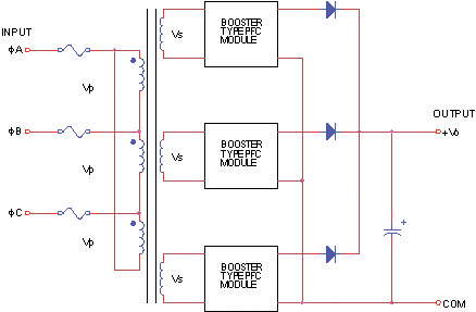 |
| Fig.(1) Topology (a). Power transformer feeds 3 non isolated PFC modules with ORed output. |
Consider the following:
(a) Existing Single Phase PFC circuits or modules may be already available in the company and can readily be used to implement a 3 Phase PFC function. This simplifies the task greatly.
(b) As per Fig. (1) the secondary voltage of the transformer (Vs) is left to the designer to determine, and thus it may be selected as high as Vo/1.4 in order to minimize the boosting action of the PFC, and thus achieve higher efficiency. For instance, if Vo (the DC bus voltage) is 250V, Vs may be chosen as high as 170VRMS. However there are some disadvantages to working at such high ratio as we shall see.
(c) This topology results in the highest efficiency when compared to all others. With the power transformer at 98% and the PFC modules at 97% an overall efficiency of 95% is practically possible.
(d) The PFC module works at fixed frequency (of choice), and this simplifies the task of attenuating EMI noise.
(e) The power transformers -albeit heavy and bulky –may be used to produce other voltages needed in the system. For instance an additional secondary may be used to generate an auxiliary power supply or a voltage for sensing the line voltage for alarms. All such secondary windings can be galvanically isolated from the primary and from each other. In other words the power transformers can have multi uses, and serve many functions not only as input to the PFC modules.
(f) The leakage inductance of the power transformer (primary to secondary) acts as an additional filter which reduces injection of EMI noise from the PFC block (the block contains 3 PFC modules) back to the utility.
(g) By the same token, this leakage inductance and the inherent characteristics of the transformer, act to buffer the PFC block from very high voltage transients riding on the input utility. MIL-STD-1399 for instance requires withstanding capability to voltage spikes of 1000V for 115V systems, and the transformer is a first line of defense for such transients.
In general, the above topology results in an excellent power factor of near unity, and the highest possible efficiency. More important however, is the fact that line current harmonics of 5% THD and 3% SHD are met, although somewhat marginally.
 |
 |
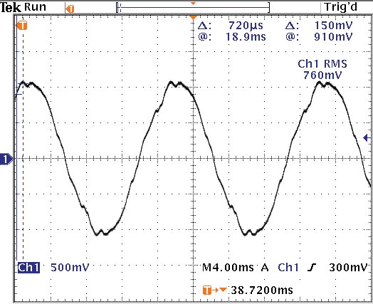 |
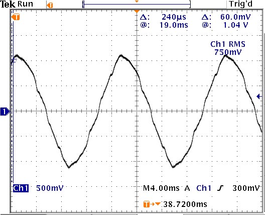
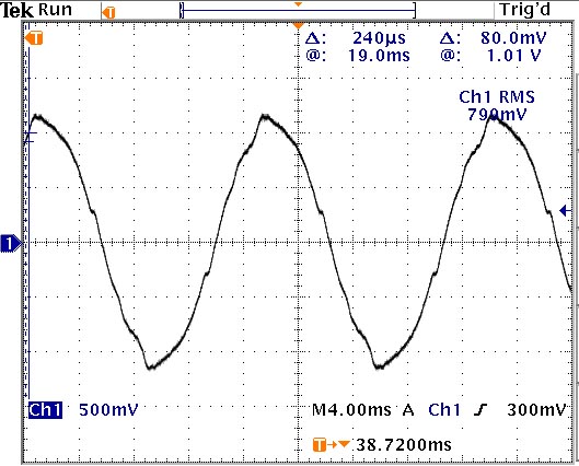
| Figure (2) Input current phase A, B and C |
Figure (2) displays the input current waveshape of the power transformer primary Phase A, B, C with an EMI filter buffering the power transformer from the utility, and a 10µf capacitor connected across each of the primaries of the power transformer.
It is important to consider the following:
(a) Distortions in the input voltage will be reflected in the input current. Experience shows that a high 3rd, 5th and 7th harmonics exist within the building voltage due to other active loads. These harmonics ranging 1-2% affect the current harmonics since the PFC does not correct for them.
(b) The power transformer itself adds to the current distortions due to non linearities in its characteristics, especially if it is designed to work at high flux densities. Up to 1.2% in current THD can come from the transformer itself.
(c) While using the popular UC3854 (A,B) PFC dedicated IC, variation from one IC to the next will contribute significantly to inconsistent PFC performance. This is not a problem if the PFC circuit is targeted to meet IEC limits, but the 5% THD and 3% SHD limits of MIL-STD-1399 are very tight, and the variation between the ICs will cause these limits to be exceeded by 1-2%. Pre-selection of ICs to pick the ones with the best performance is possible, but it is time consuming and costly.
It was found that the higher the line frequency current ratio compared to the high frequency current in the input of the PFC, the lower will be the current harmonics overall. One way to achieve this is by increasing operational frequency of the PFC so as to reduce high frequency current ripple. A second more effective method is to increase the input line frequency current of the PFC by lowering the input voltage Vs. In our case, reducing Vs from 170VRMS to 140VRMS, enhanced the performance of the PFC modules, with a minute effect on efficiency. Admittedly the PFC has to work a bit harder to boost 140V to 250VDC than where 170VRMS is boosted to that level. Further, shaping of the voltage error amplified performance of the UC3854 (A,B) by changes in the compensation network, resulted in additional enhancement and in less dependency on the IC performance. With all of the above enhancements, and with the input voltage near perfect sinewave, meeting MIL-STD-1399 limits is guaranteed.
The volumetric, and weight parameters of this topology are as follows:
 |
| Fig.(3a) Single non isolated PFC Module accepts and delivers 250VDC 1KW. 130-170Vrms. |
 |
| Fig (3b) One block of 3 non-isolated PFC modules can deliver 250VDC up to 3KW. Was tested up to 4.5KW output. |
The PFC block containing 3 individual PFC modules
[as shown in Fig (3)] measures 10.5” x 5” x 5” and thus 262.5 cubic inch in volume. Measured weight was 7.4lbs. This block is capable of delivering 3KW easily. The same parameters for the 3KW Power Transformer are 9” x 7” x 4.5” resulting in a volume of 283.5 cubic inch and 46 lbs in weight. Therefore the overall volume and weight parameters of this approach are 546 cubic inch, and 53.4 lbs.
III. Isolated Output PFC Solutions
Producing an isolated DC output from a 3 Phase Delta Utility is also possible by use of 3 Single Phase isolated output PFC modules as shown in Fig. (4). The output of the modules are then ORed to create one common DC bus. In the case of MIL-STD-1399 type I shipboard utility, the input is 115V line to line Delta 60Hz. The DC needed in our application was 250V to energize an inverter module which was designed to deliver an output of 115V 400Hz Single Phase. This topology is flexible, but for practical reasons, it should be limited to 250Vrms input and no more than 400V output. These limits result from FET transistor availability in the high voltage range, and the fact that the topology is actually single ended flyback. This topology is also inherently not suitable for higher power levels than 1KW per module.
 |
| Fig(4) Topology(b). 3 Isolated output PFC modules Ored at the output. Each employs Flyback topology |
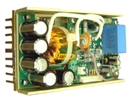
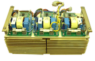
The circuit shown in Fig.(4) contains 3 individual isolated PFC modules, each is rated to 1KW output power. The combined block can therefore deliver 3KW output. The circuit for each module is a classical flyback, and the power stage employs a single 40A 600V FET transistor. The secondary side of the transformer is designed to generate 250VDC. The logic circuit is a classical PFC circuit employing UC3854A which was used in the non isolated PFC as well. An operational frequency of 40KHz was chosen as a good compromise considering the flyback power transformer size, acceptable switching losses in the power switch, and power loss in the ultra fast output rectifiers. A picture of the 3 PFC modules is shown in Fig. (5).
The following considerations apply:
(a) A flyback topology may be designed to work in the continuous (CCM) or discontinuous (DCM) conduction mode. In our case CCM was chosen in order to limit peak current amplitude, although DCM would have been better for EMI. Should the individual PFC be limited to only 300W, a DCM approach will be applicable.
(b) Output rectifier recovery in the form of high frequency ringing is a major source of EMI pollution and power loss, even if ultra fast (and soft recovery) rectifiers (of 35nS) are used. In retrospect it is advised to consider Silicon Carbide diodes. Up to 3% higher efficiency can be realized with the SiC diodes, but more importantly the dominant benefit is substantial reduction in the EMI noise, and significant decrease in stress level for the power transistor.
(c) This topology is limited in power capability due to power transistor limitation, and the size of the power transformer. Using this flyback scheme for power higher than 1KW per module (3kW for the block) is not usually practical.
(d) As always in flyback circuits, the power transformer design, geometry, and construction are critical. It is paramount to minimize the primary to secondary leakage inductance to avoid high voltage spikes at the primary side at the turn off time. These spikes will destroy the power transistor if not clamped or snubbed. The clamping though entails significant power loss and up to a 1% loss of efficiency.
 |
| Fig (5a) Single isolated PFC module delivers 1KW output from line to line voltage. The isolated output is 250VDC |
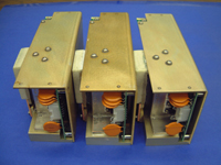 |
| Fig (5b) 3 Isolated output PFC made of 3 modules. This combination will connect to Delta input of 115V line to line and deliver one 250VDC output to 3KW |
The need to critically reduce leakage inductance imposes severe constraints on the power transformer. A “Sandwich” interleaved winding construction method with the secondary split between primary sections was used to achieve better coupling and low leakage. Measured leakage inductance was 5µH on this EE cored transformer which in its finished form resembles a cube of 2” x 2” x 2” in size.
Further consideration was given to skin effect in the winding and heat buildup in the transformer. Multiple strands of #30 wire were used for the winding, and encapsulation with thermally conductive epoxy was applied to transfer the heat out of the core and the windings to a heatsink.
All of the above issues pertaining to the transformer design signify the complexity of this approach, but this is not all. A high frequency noise from switching, and strong magnetic field from the gapped transformer cause adverse parasitic effects in the logic, and result in instability (and jittery performance), unless addressed properly. The layout of the logic section is also critical. Ground loops must be avoided by careful layout, and the logic circuit needs to be physically located as far from the power stage as possible.
When 3 isolated output PFC modules are arranged as a block the overall size will be 8.5” x 10” x 5”, i.e. 425 inch cube, and the overall weight is only 18lbs. In comparison, the non isolated PFC-transformer combination as mentioned was 546 cubic inch, and 53.4lbs. Clearly, for the 3kW case, the isolated PFC approach offers very noticeable advantages in weight, and to a much lesser extent in volume.
Not so however is the case with efficiency. The measured efficiency of the isolated PFC block is 90.7%.
One can however safely assume that by using SiC diodes an increase in efficiency of 3% will occur. The performance of this topology in terms of input current harmonics is generally good and only slightly worse than that of the first topology. The block of 3 isolated PFC modules, buffered from the Delta input (115V/60Hz line to line) with a (multi stage) EMI filter, was able to comply with MIL-STD-1399 and MIL-STD-461 (for EMI) and fulfill all its objectives. Still, reliability, efficiency, and EMI issues make this topology inferior to the prior one. However in applications limited to 3kW, and where weight (and to a lesser degree volume) is very critical, this isolated PFC approach is very advantageous.
IV. 3 Phase Single Stage Multi Resonant, Buck Type Topology
It is possible to generate a regulated DC bus from one stage PFC circuit which can meet the current harmonics criteria set forth. Galvanic Isolation can then be achieved by either an input power transformer or an output DC to DC converter. In essence this is a variation on the theme of the first topology.
However, while that topology mandates the use of a front-end power transformer (to achieve isolation and 3 separate secondaries); This third topology makes the use of the transformer optional, being that this single stage PFC circuit works directly with Delta input. Therefore, the isolation can be achieved either by the use of DC-DC converter following it, or by an input transformer. Reliability, cost, and efficiency criteria will promote the choice of the input transformer over the DC –DC converter, to achieve isolation. The reasons are obvious: While the power transformer efficiency is 97-98% that of the DC-DC converter will provide 90-92% at best. Further, the transformer allows us to step the 115V line to line voltage to the desired value, thus allowing higher efficiency in the PFC. Its leakage inductance will assist EMI filtering, and also reduce susceptibility to line voltage spikes.
By comparison, the use of a DC-DC converter working at say 100KHz will result smaller volume and weight, but it will produce markedly higher EMI common mode and differential mode noise.
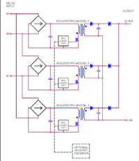
The 3 Phase resonant [zero current switching] Buck topology PFC circuit, features a single switch control, constant On-time and varied Off time PWM. It produces a non isolated DC output, and works directly from Delta input. As the name implies, a Buck method is used in lieu of the traditional boost circuit prevalent in most PFC circuits. The use of a Buck in this scheme reduces the number of inductors needed. The references provide [1-7] much in-depth information about this topology which is described in the schematic diagram of Fig (6).
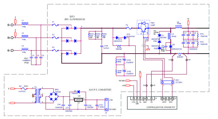 |
| Fig(6) Schematic of single stage, 3Phase resonant buck PFC circuit capable of connecting to Delta utility and delivering DC Output Voltage. |
g) The control circuit which provides the constant on-time of 7µS is relatively simple using UC3843 IC as a voltage error amplifier and CD4047 as a monostable multi-vibrator.
(h) The voltage or current stress levels on some of the power components are extremely high, and as a result the IGBT used was rated 1200V 100A. The following stress levels associated with his topology should be expected with 3KW load in a setup where the input is 208Vrms and the output 200VDC. These numbers are derived by simulation since we did not compile them at the time from the actual breadboard.
IGBT peak voltage: 633V
IGBT peak current: 68A
IGBT average current: 14.3A
C1-C3 rms current: 16.3A
C1-C3 peak voltage: 362V
BR1 peak current: 68A
BR1 average current per diode: 5.1A
D2 peak voltage: 420V
D2 peak current: 14.6A
D2 average current: 7.5A
D3 peak voltage: 646V (note: normally D3 does not carry any current) D14-D15
Peak voltage (total): 647V (note: normally D3 does not carry any current)
The purpose of D3 and D14-D15 is to protect against a low energy resonance, which happens at light load when the switching frequency crosses the resonant frequency of the input inductors and capacitors (C1-3). This is the point when the worst-case voltage stress happens. The voltage stress at that point depends on the resistance of R104 (39k/3W). The peak voltage with that resistor is around 800-900V. It is possible that the voltage stress can be reduced by allowing more dissipation in R104.
(i) The capacitor C5 conducts very high current at resonation and thus has to be of very low ESR and high current capability at high frequency. A relatively large polypropylene capacitor is needed.
(j) Of particular importance is the criticality of the situation whereas the operating frequency at the low end nears that of the resonance frequency of the input line filters (L1-L3 with C1-C3). If these frequencies become equal, circuit failure will occur.
Therefore, one must guarantee by design that at light load, the operational frequency does not drop to or below the resonant frequency of the line L-C components. It is advisable to stop switching when this critical situation is approached, and go to burst-mode instead. This point cannot be emphasized any further.
(k) The line inductors L1-L3 must be able to handle the line current without saturating while also their inductance must be relatively high (1mH in our case).
In general, it seems clear that in the range of 3kW this topology provides no advantage over the previously mentioned two. While the isolation stage is considered, this topology is also at a disadvantage from volume and weight points of view, and it is rather problematic from an EMI perspective due to the wide rage frequency variation.
Further, its design is not simple even though the power circuit as well as the logic seems very simple. The resonation effects and the high frequency at high load, cause stress factors on the power components, that are far greater than any conventional PFC circuit.
V. Summary
It is clear from this comparison that in the 3KW level, if efficiency and EMI are the dominant criteria, the first topology (3 non isolated PFC modules buffered from the utility by a power transformer is most advantageous. If however weight and volume are most important, the second topology (3 isolated output, flyback type circuit) is a better choice. The last topology discussed in the paper (Resonant Buck – preceded by a power transformer, or followed by a DC-DC converter) does not in fact provide any advantage.
Acknowledgement:
The author wishes to thank Dr. Richard Redl of ELFI S.A. for his major contribution in the design and simulation of the circuits discussed in this article.
To Download the Article in PDF Format CLICK HERE